|![[Search]](https://talks.cam.ac.uk/images/search.gif?1209136071) |
|![[A-Z Index]](https://talks.cam.ac.uk/images/az.gif?1209136071) |
|![[Contact]](https://talks.cam.ac.uk/images/contact.gif?1209136071)
| COOKIES: By using this website you agree that we can place Google Analytics Cookies on your device for performance monitoring. | ![[Talks.cam]](https://talks.cam.ac.uk/images/talkslogosmall.gif?1209136071) |
University of Cambridge > Talks.cam > Semiconductor Physics Group Seminars > Cutting graphene with an AFM: device lithography in under a minute
Cutting graphene with an AFM: device lithography in under a minuteAdd to your list(s) Download to your calendar using vCal
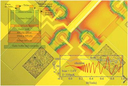
If you have a question about this talk, please contact afw24. Graphene was first isolated six years ago, and has since generated enormous interest due to its potential for electronics applications. It is intrinsically conducting, with no band gap, but may be patterned to confine conduction; room temperature transistor behaviour requires graphene ribbons only a few nanometres wide, at or beyond the limits of conventional lithography and etching processes. A potential alternative uses the sharp point of a scanning probe microscope to tailor the graphene flake. In this work a charged AFM tip has been used to cut patterns on few and single layer graphene with feature sizes as small as 5 nm. In addition to these results, this talk will present analysis used to derive a molecular mechanism for the removal of carbon, discussing in particular the role of water and an unstable solid carbon oxide. Thermal annealing also revealed the presence of water beneath flakes, which influences their transport behaviour. This talk is part of the Semiconductor Physics Group Seminars series. This talk is included in these lists:
Note that ex-directory lists are not shown. |
Other listsPublic talk: Duncan Watts Interdisciplinary Design: Debates and Seminars Software InnovationOther talksMarket Socialism and Community Rating in Health Insurance Babraham Distinguished Lecture - Endoplasmic reticulum turnover via selective autophagy Description: TIE proteins: chemical harpoons of Gram-positive bacteria The MMHT view of the proton Genomic Approaches to Cancer Cambridge-Lausanne Workshop 2018 - Day 2 Glucagon like peptide-1 receptor - a possible role for beta cell physiology in susceptibility to autoimmune diabetes Unbiased Estimation of the Eigenvalues of Large Implicit Matrices Sneks long balus Loss and damage: Insights from the front lines in Bangladesh |

 Mr Philip Scard (Semiconductor Physics Group, Cambridge)
 Monday 31 May 2010, 14:15-15:15