|![[Search]](https://talks.cam.ac.uk/images/search.gif?1209136071) |
|![[A-Z Index]](https://talks.cam.ac.uk/images/az.gif?1209136071) |
|![[Contact]](https://talks.cam.ac.uk/images/contact.gif?1209136071)
| COOKIES: By using this website you agree that we can place Google Analytics Cookies on your device for performance monitoring. | ![[Talks.cam]](https://talks.cam.ac.uk/images/talkslogosmall.gif?1209136071) |
University of Cambridge > Talks.cam > Electron Microscopy Group Seminars > Exploring the world with high angular resolution electron backscatter diffraction (HR-EBSD)
Exploring the world with high angular resolution electron backscatter diffraction (HR-EBSD)Add to your list(s) Download to your calendar using vCal
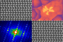
If you have a question about this talk, please contact Duncan Johnstone. The advent of precise, high fidelity and automated tools for electron microscopy provides exciting new opportunities to engineer the world around us. In particular we can carefully measure, characterise and understand the interplay of microstructure and properties to drive mechanistic understanding at a wide range of length scales. One such technique employed routinely within the scanning electron microscope (SEM) is electron backscatter diffraction (EBSD). Diffraction patterns are captured as the electron probe is scanned across the surface of a well-polished crystalline sample and maps of microstructure, including distributions of crystal orientation, morphology and phase can be generated easily with commercially available software tools based upon the Hough transform and typical crystal misorientation precision is 0.5 degrees. The typical spatial resolution of the technique is 100nm. For an even deeper understanding of the microstructure-performance-properties paradigm, the diffraction patterns can be analysed using sophisticated image processing algorithms to extract higher precision information concerning misorientation within grains and ultimately elastic strain (and through Hooke’s law, stress). This is achieved through cross correlation of two or more diffraction patterns, providing increased sensitivity of two orders of magnitude, and enables (deviatoric) elastic strains of 1E-4 and lattice misorientations of 0.006 degrees (~1E-4 rads) to be measured. In this talk, I will introduce the overall technique including the recent remapping approach and outline our approaches to understand precision, accuracy and sensitivity within grains and near grain boundaries. This will be followed by a few case studies including: a combined study with high spatial resolution digital image correlation to recover components of the complete deformation gradient tensor, F; measurement of geometrically necessary and total dislocation density in metals and semiconductors; and finally an examination of dislocation pile-ups near grain boundaries in titanium. This talk is part of the Electron Microscopy Group Seminars series. This talk is included in these lists:
Note that ex-directory lists are not shown. |
Other listsFoster Talks Cambridge Countercultural Studies Research Group Soc Doc Soc Computer Laboratory Opera Group Seminars Inspirational Women in Engineering Talk Series Tencent Talk: Fast and Furious Explore the Ever-changing Digital ChinaOther talksScience Makers: multispectral imaging with Raspberry Pi Enhanced Decision Making in Drug Discovery Adding turbulent convection to geostrophic circulation: insights into ocean heat transport “It’s like they’re speaking a different language!” Investigating an accidental resistance to school mathematics reform What You Don't Know About God |

 Ben Britton,Department of Materials, Imperial College London

 Monday 18 January 2016, 14:00-15:00