3-dimensional dislocation imaging in the electron micoscope: Analysis of delamination in GaN devices
Add to your list(s)
Download to your calendar using vCal
If you have a question about this talk, please contact Edmund Ward.
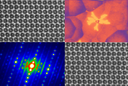
This talk will examine the technique of three-dimensional mapping of dislocations in the transmission electron microscope (TEM) by combining weak-beam dark-field imaging with tomography. Even with a relatively simple TEM , we show that it is possible to recover the vast majority of dislocations with varying degrees of fidelity. We demonstrate this by examining the microstructure of plastically relaxed p-type gallium nitride that plays host to a variety of dislocation types. We show that the technique works well for dislocations spaced above 10nm apart, while below this it is difficult to recover dislocations confidently. Future developments and ideas will be discussed.
This talk is part of the Electron Microscopy Group Seminars series.
This talk is included in these lists:
Note that ex-directory lists are not shown.
|
![[Search]](https://talks.cam.ac.uk/images/search.gif?1209136071) |
|![[A-Z Index]](https://talks.cam.ac.uk/images/az.gif?1209136071) |
|![[Contact]](https://talks.cam.ac.uk/images/contact.gif?1209136071)
![[Talks.cam]](https://talks.cam.ac.uk/images/talkslogosmall.gif?1209136071)

 Jonathan S Barnard, Department of Materials Science and Metallurgy, University of Cambridge
 Tuesday 30 May 2006, 15:00-16:00