|![[Search]](http://talks.cam.ac.uk/images/search.gif?1209136071) |
|![[A-Z Index]](http://talks.cam.ac.uk/images/az.gif?1209136071) |
|![[Contact]](http://talks.cam.ac.uk/images/contact.gif?1209136071)
| COOKIES: By using this website you agree that we can place Google Analytics Cookies on your device for performance monitoring. | ![[Talks.cam]](http://talks.cam.ac.uk/images/talkslogosmall.gif?1209136071) |
University of Cambridge > Talks.cam > Electron Microscopy Group Seminars > Kinetic measurements during the nucleation and growth of Si and Ge
Kinetic measurements during the nucleation and growth of Si and GeAdd to your list(s) Download to your calendar using vCal
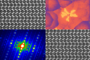
If you have a question about this talk, please contact Nathan Church. By carrying out chemical vapour deposition of semiconductors in the presence of small particles of a catalytic material, it is possible to grow wirelike structures microns long and below 100nm in diameter. Such nanowires have interesting electronic properties and have already been incorporated into functional devices. Even more applications can be envisaged for branched nanowires or nanowires grown epitaxially at precise locations over an entire wafer. In this presentation we will discuss the growth of epitaxial nanowires in Si and Ge using Au as the catalyst, focusing on the kinetic processes that influence nucleation and final shape. Growth takes place in an environmental TEM , which has capabilities both for evaporating Au onto a clean Si substrate, and for introducing the precursor gases while the sample remains under observation. In situ video rate observations allow us to measure nucleation events and nanowire growth rates, examine the catalyst structure directly, and determine the effects of changes in growth environment on wire shapes. We will focus in particular on the factors that affect shape and the reliability of nucleation, and consider how the in situ results may help in tailoring wire structures for particular applications. This talk is part of the Electron Microscopy Group Seminars series. This talk is included in these lists:
Note that ex-directory lists are not shown. |
Other listsmiddle east studies Foster Talks Synthetic Chemistry Research Interest GroupOther talksA transmissible RNA pathway in honeybees Lipschitz Global Optimization All-resolutions inference for brain imaging Finding the past: Medieval Coin Finds at the Fitzwilliam Museum Part IIB Poster Presentations Beyond crazy: Rationality, irrationality, and conspiracy theory Single Cell Seminars (August) Cambridge-Lausanne Workshop 2018 - Day 2 The Anne McLaren Lecture: CRISPR-Cas Gene Editing: Biology, Technology and Ethics EU LIFE Lecture - "Histone Chaperones Maintain Cell Fates and Antagonize Reprogramming in C. elegans and Human Cells" 'Politics in Uncertain Times: What will the world look like in 2050 and how do you know? Poland, Europe, Freedom: A Personal Reflection on the Last 40 Years |

 Frances M Ross, IBM T J Watson Research Center
 Tuesday 06 February 2007, 15:00-16:00