|![[Search]](http://talks.cam.ac.uk/images/search.gif?1209136071) |
|![[A-Z Index]](http://talks.cam.ac.uk/images/az.gif?1209136071) |
|![[Contact]](http://talks.cam.ac.uk/images/contact.gif?1209136071)
| COOKIES: By using this website you agree that we can place Google Analytics Cookies on your device for performance monitoring. | ![[Talks.cam]](http://talks.cam.ac.uk/images/talkslogosmall.gif?1209136071) |
University of Cambridge > Talks.cam > Electron Microscopy Group Seminars > Recent advances in specimen preparation and manipulation technology for SEM/FIB and TEM
Recent advances in specimen preparation and manipulation technology for SEM/FIB and TEMAdd to your list(s) Download to your calendar using vCal
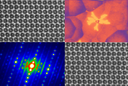
If you have a question about this talk, please contact Edmund Ward. The use of Field Emission Guns on modern TEM and SEM instrumentation has led to significant improvements in imaging and analytical performance. Specimens have also grown in diversity and complexity demanding more advanced specimen preparation technologies. Typical specimen preparation starts by choosing a suitable site from the bulk specimen. Care has to be taken at every stage to minimise the damage introduced to the specimen from cutting, grinding or polishing. The next stage involves dimple grinding of the specimen which is performed to reduce the time taken to Ion Mill the specimen to perforation. During Ion Milling the energy, current, angle and temperature will affect the final result. With many new materials phase changes can result if the temperature is not controlled. The ultimate speed of ion milling may well be at the detriment to the sample. Before examination of the specimen in the microscope it is important to remove any hydrocarbon contamination from both the specimen and holder. Typically both are cleaned prior to insertion in the electron microscope using a plasma cleaner. Removal of this contamination will prevent the deposition of carbon on the sample during imaging or analysis. New Preparation Technologies such as FIB allow the preparation of very site specific areas of the specimen. The ultimate specimen however can possess some features which are not ideal for high-resolution or analytical microscopy. These defects include curtaining and amorphous contamination which affect the physical and electrical properties. Using a focused low energy argon ion source to scan and image the lamella, amorphous material can be removed. The ultimate sample is then suitable for characterisation by TEM . Imaging of specimens in STEM using a HAADF detector with a DQE in excess of 98 per cent results in single electron detection efficiency. In addition, combining STEM with tomography allows the three-dimensional reconstruction of Materials Science samples without significant contributions from diffraction contrast during data collection. A high tilt capability combined with a large field of view in a narrow gap pole piece is now necessary. Biasing of samples during tilting and acquiring electron holograms now allows the reconstruction of electric fields in semiconductor device samples in three dimensions. Specimen Preparation Technology for SEM has also become more complex. Field Emission SEMs have high resolution at low accelerating voltages. For EBSD the sample surface has to remain free of artefacts at the atomic level. Cleaving, polishing and cleaning of the specimen surface is no longer a viable method. Combining technologies such as Ion Beam Etching, Reactive Ion Beam Etching, Plasma Cleaning and Coating in a single vacuum chamber reduces specimen artefacts. Using the correct combination of technologies can result in optimising representative data collection from specimens. This talk is part of the Electron Microscopy Group Seminars series. This talk is included in these lists:
Note that ex-directory lists are not shown. |
Other listsAcoustics Lab Seminars Europe East and West: Film, History, and Mourning Film Screenings and TalksOther talksTBC Martin Roth: »Widerrede!« Transcriptional control of pluripotent stem cell fate by the Nucleosome Remodelling and Deacetylation (NuRD) complex Findings from Studies of Virtual Reality Sketching The Hopkins Lecture 2018 - mTOR and Lysosomes in Growth Control MicroRNAs as circulating biomarkers in cancer The frequency of ‘America’ in America Microtubule Modulation of Myocyte Mechanics Katie Field - Symbiotic options for the conquest of land Stereodivergent Catalysis, Strategies and Tactics Towards Secondary Metabolites as enabling tools for the Study of Natural Products Biology Cambridge - Corporate Finance Theory Symposium September 2017 - Day 1 Biopolymers for photonics - painting opals with water and light |

 Alan C Robins , E A Fischione Instruments Inc
 Tuesday 25 April 2006, 15:00-16:00