|![[Search]](http://talks.cam.ac.uk/images/search.gif?1209136071) |
|![[A-Z Index]](http://talks.cam.ac.uk/images/az.gif?1209136071) |
|![[Contact]](http://talks.cam.ac.uk/images/contact.gif?1209136071)
| COOKIES: By using this website you agree that we can place Google Analytics Cookies on your device for performance monitoring. | ![[Talks.cam]](http://talks.cam.ac.uk/images/talkslogosmall.gif?1209136071) |
University of Cambridge > Talks.cam > Electron Microscopy Group Seminars > Failure analysis of semiconductor lasers
Failure analysis of semiconductor lasersAdd to your list(s) Download to your calendar using vCal
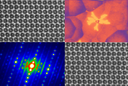
If you have a question about this talk, please contact Edmund Ward. Fully processed wafers of III -V semiconductor lasers have a potential value of tens of thousands of pounds; yield and reliability issues can therefore be very expensive. The most challenging problems occur when defects or processing issues which are introduced during fabrication are latent in the device; performance is good upon initial test, but the devices degrade during burn in or an accelerated life test trial. This talk describes the type of failure analysis study which is needed to solve these issues, using examples from work done at Bookham Technology, Caswell. Specimen preparation is challenging, requiring analysis of specific sites on individual devices, and usually several types of analysis are used, including electroluminescence, SEM , FIB and TEM - often on the same device. Results of an accelerated life test study of InAs/GaAs quantum dot lasers are also presented. These indicate that quantum dot material is inherently resistant to defect propagation – much more so than devices which use quantum wells. This talk is part of the Electron Microscopy Group Seminars series. This talk is included in these lists:
Note that ex-directory lists are not shown. |
Other listsCambridge Neuroscience Seminar, 2011 Book Launches Special Lecture Series: THE NATURAL COOK: A THEORY OF HUMAN EVOLUTIONOther talksCambridge Rare Disease Summit 2017 Identifying new gene regulating networks in immune cells High-Dimensional Collocation for Lognormal Diffusion Problems Microsporidia: diverse, opportunistic and pervasive pathogens CPGJ Academic Seminar: "The teaching professions in the context of globalisation: A systematic literature review" CANCELLED: The Loxbridge Triangle: Integrating the East-West Arch into the London Mega-region Single Cell Seminars (November) TBC Towards a whole brain model of perceptual learning Vision Journal Club: feedforward vs back in figure ground segmentation How to Deploy Psychometrics Successfully in an Organisation Advanced NMR applications |

 Richard Beanland, Bookham Technology, Caswell
 Thursday 26 July 2007, 15:00-16:00