|![[Search]](http://talks.cam.ac.uk/images/search.gif?1209136071) |
|![[A-Z Index]](http://talks.cam.ac.uk/images/az.gif?1209136071) |
|![[Contact]](http://talks.cam.ac.uk/images/contact.gif?1209136071)
| COOKIES: By using this website you agree that we can place Google Analytics Cookies on your device for performance monitoring. | ![[Talks.cam]](http://talks.cam.ac.uk/images/talkslogosmall.gif?1209136071) |
University of Cambridge > Talks.cam > Electron Microscopy Group Seminars > Proof-of-concept of multi-electron-beam system
Proof-of-concept of multi-electron-beam systemAdd to your list(s) Download to your calendar using vCal
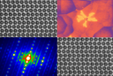
If you have a question about this talk, please contact Edmund Ward. In the fields of semiconductor device manufacturing and inspection, a multi-electron-beam system is one of the most promising candidates for both high resolution and high throughput. In the multi-electron-beam system, uniformity of optical property, individual blanking control, and accurate calibration of beam position and dose are important. Multi-electron-beam systems can be roughly divided into three types: 1) multi-column with multi-source, 2) single-column with multi-source, and 3) single-column with single-source. We adopted single-column system with single-column because we thought that this system is simpler than the others and has an advantage in stability and fewer calibrations. In our system, the beam, which emitted from LaB6 single electron source with an acceleration voltage of 50 kV, is collimated by the collimator lens to illuminate multi-source-module (MSM). The MSM consists of three devices, aperture array (AA: beam dividing aperture), static lens array (SLA: focusing lens for each divided beam to form the intermediate source images), and blanker array (BLA: pairs of electrodes as blankers for each focused beam), and forms 1024 multiple beams. The intermediate source image at BLA is demagnified by the projection optics. The projection optics is constructed by double lens-doublet for low-distorted projection. In the projection optics, the blanking aperture and deflector are installed. The beam, which is applied blanking voltage, is cut off at the blanking aperture, and the beams, which passed the blanking aperture, are deflected together. We verified the actions of SLA and BLA , and successfully formed 1024 multiple beams. Moreover, some pattern delineations were executed as verification of individual beam control with several beams among the 1024 beams. It remains the measurement of optical property and verification of calibration of beam position and dose. With those results, it will be verified that our multi-beam system has potential use in inspection or lithography process of semiconductor device production. This talk is part of the Electron Microscopy Group Seminars series. This talk is included in these lists:
Note that ex-directory lists are not shown. |
Other listsBritish Science Association McDonald Lectures & Seminars Connecting with Collections SymposiumOther talksA feast of languages: multilingualism in neuro-typical and atypical populations Development of machine learning based approaches for identifying new drug targets Protein targeting within the chloroplast: a cell-biological view of starch biosynthesis Modeling and understanding of Quaternary climate cycles The spin evolution of supermassive black holes Computing knot Floer homology Picturing the Heart in 2020 Networks, resilience and complexity "The integrated stress response – a double edged sword in skeletal development and disease" The Digital Doctor: Hope, Hype, and Harm at the Dawn of Medicine’s Computer Age St Catharine’s Political Economy Seminar - ‘Global Imbalances and Greece's Exit from the Crisis’ by Dimitrios Tsomocos |

 Osamu Kamimura, Central Research Laboartory, Hitachi, Japan
 Thursday 27 July 2006, 11:30-12:30