|![[Search]](http://talks.cam.ac.uk/images/search.gif?1209136071) |
|![[A-Z Index]](http://talks.cam.ac.uk/images/az.gif?1209136071) |
|![[Contact]](http://talks.cam.ac.uk/images/contact.gif?1209136071)
| COOKIES: By using this website you agree that we can place Google Analytics Cookies on your device for performance monitoring. | ![[Talks.cam]](http://talks.cam.ac.uk/images/talkslogosmall.gif?1209136071) |
University of Cambridge > Talks.cam > HREM > Field mapping of semiconductor devices with 1 nm-scale resolution by off axis electron holography
Field mapping of semiconductor devices with 1 nm-scale resolution by off axis electron holographyAdd to your list(s) Download to your calendar using vCal
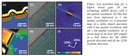
If you have a question about this talk, please contact Caterina Ducati. This talk has been canceled/deleted Off-axis electron holography is a powerful transmission electron microscopy (TEM) based technique that uses an electron biprism to interfere an electron beam that has passed through a region of interest with a beam that has passed through only vacuum. From the resulting interference pattern, also known as the hologram, a phase image of the specimen can be reconstructed. As the phase of an electron is sensitive to the electrostatic potential, strain or magnetic fields in or around the specimen, then electron holography can be used to measure these properties with nm-scale resolution. In this talk we will show some examples of electron holography as has been applied to different types of specimens in an applied semiconductor environment for both active dopant and strain mapping. Figure 1(a) shows a potential map of a 28-nm-gate technology nMOS high-k metal gate device acquired using Lorentz mode off-axis electron holography with a spatial resolution of 6 nm. However, the resolution is unsuitable to visualise the active dopants that are directly under the gate. By obtaining a potential map with 1 nm spatial resolution (b) it is now possible to see the position of these active dopants to help understand the electrical properties of the device. Figure 1© shows a potential map of highly doped boron delta layers each spaced by 3.5 nm. For clarity, the map has been overlaid onto a TEM image to show the position of the delta layers. Using conventional Lorentz holography with a spatial resolution of 6 nm, these layers were not resolved. (d) In the first successful quantification of these layers, we acquired potential maps with 1 nm spatial resolution and the active dopant concentration was found to be consistent with the solubility limit of boron in silicon. We will also show results that we have obtained using dark field electron holography to provide strain maps of an epitaxially grown InAs QD in InP with 1 nm spatial resolution. Figure 1(e) shows the map for the (004) growth direction with 1 nm spatial resolution. A value of 6% strain is measured in the dot, which is consistent with simulations. (f) No strain is measured in the (220) in plane direction, as the QD is in perfect epitaxy with the InP substrate. We will present some examples of electron holography used to solve materials science problems. We will discuss the limitations of the technique and we will show problems that are typically encountered during specimen preparation. We will also compare our holography results with those acquired using other TEM - based techniques such as EELS and nanobeam diffraction. Finally, as the dimensions of semiconductor devices are reduced to the atomic scale we will discuss the future prospects for electron holography. This talk is part of the HREM series. This talk is included in these lists:This talk is not included in any other list Note that ex-directory lists are not shown. |
Other listsCambridge Geotechnical Society Seminar Series Nonlinear Waves Automation and how it can help youOther talksThe Digital Doctor: Hope, Hype, and Harm at the Dawn of Medicine’s Computer Age Visual Analytics for High-Dimensional Data Exploration and Engineering Design What constitutes 'discrimination' in everyday talk? Argumentative lines and the social representations of discrimination Microsporidia: diverse, opportunistic and pervasive pathogens Making Refuge: Academics at Risk Behavioural phenotypes of children born preterm: what we know and future research avenues Dynamics of Phenotypic and Genomic Evolution in a Long-Term Experiment with E. coli Throwing light on organocatalysis: new opportunities in enantioselective synthesis Coatable photovoltaics (Title t o be confirmed) Protein Folding, Evolution and Interactions Symposium Prof Chris Rapley (UCL): Polar Climates |


 Thursday 13 October 2011, 15:00-16:00