|![[Search]](http://talks.cam.ac.uk/images/search.gif?1209136071) |
|![[A-Z Index]](http://talks.cam.ac.uk/images/az.gif?1209136071) |
|![[Contact]](http://talks.cam.ac.uk/images/contact.gif?1209136071)
| COOKIES: By using this website you agree that we can place Google Analytics Cookies on your device for performance monitoring. | ![[Talks.cam]](http://talks.cam.ac.uk/images/talkslogosmall.gif?1209136071) |
University of Cambridge > Talks.cam > CAPE Advanced Technology Lecture Series > Semiconductor nanowires: harder, better, faster, stronger
Semiconductor nanowires: harder, better, faster, strongerAdd to your list(s) Download to your calendar using vCal
If you have a question about this talk, please contact Dr Mark Leadbeater. For online access register at: https://eng-cam.zoom.us/j/84761376876. Abstract III –V nanowires exhibit unique properties that don’t appear in their bulk counterparts: the ability to combine novel combinations of lattice-mismatched materials, more efficient light absorption and light emission, waveguiding, more efficient charge transport, high Young’s modulus, high elastic failure limit, reduced materials usage and lower temperature manufacturing conditions. These advantages translate to more efficient, faster, stronger and more environmentally-friendly devices. The non-planar nature of free-standing III –V nanowires therefore creates new opportunities for electronic and optoelectronic devices, but it also necessitates new strategies for nanowire growth and integration. In this presentation, routes for nanowire growth and integration will be discussed. Firstly, the growth parameters for catalyst-free III –nitride nanowire growth by metalorganic vapour phase epitaxy will be discussed. Surface modifications and passivation, achieved either during growth or post-growth, are also necessary for achieving reproducible device performance. We will present the development of a multiplexer chip capable of addressing single-nanowire transistors in arrays. Nanowires, deterministically positioned on the multiplexer by transfer-printing, exhibited reproducible electrical behaviour and high device yield. The multiplexer’s ability to operate from room temperature down to milliKelvin temperatures enables the study of quantum phenomena in multiple and interconnected nanowire devices. A promising route towards flexible electronics involves embedding nanowires in a transparent polymer host matrix. By judicious choice of polymer type and deposition conditions, the encapsulated nanowire array preserves the as-grown orientation of the nanowires and can be removed from the rigid growth substrate, creating a flexible and robust device while permitting re-use of the substrate for subsequent growths. This process technique has been used to create flexible terahertz modulator devices based on arrays of aligned GaAs nanowires. Biography Hannah Joyce is Professor in low-dimensional electronics at the University of Cambridge. She completed her PhD at the Australian National University and a postdoc at the University of Oxford. After joining Cambridge in 2013, she established the “Electronic and Photonic Nanodevices Group” in Division B. Her group focusses on the development of novel nanomaterials for applications in photonics and electronics. Her interests span the growth of nanowires, terahertz spectroscopy for contact-free characterisation of nanomaterials, and the development of new nanomaterial-enabled devices such as photodetectors and terahertz photonic modulators. This talk is part of the CAPE Advanced Technology Lecture Series series. This talk is included in these lists:
Note that ex-directory lists are not shown. |
Other listsRema 2020 eSCAMPS 2020 Ancient Near East Seminar SeriesOther talksEisenstein Series and Ensemble Averages in Holography Hypergroup orbifolds of vertex operator algebras LCLU Coffee Summeries Learning Operators From Data; Applications to Inverse Problems and Constitutive Modeling - Bayesian Inversion and Surrogate Modeling Population structure and effects of consanguinity on complex disease in British South Asians |

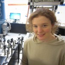
 Professor Hannah Joyce, University of Cambridge
 Tuesday 20 June 2023, 14:00-15:00