| COOKIES: By using this website you agree that we can place Google Analytics Cookies on your device for performance monitoring. | ![[Talks.cam]](http://talks.cam.ac.uk/images/talkslogosmall.gif?1209136071) |
University of Cambridge > Talks.cam > Materials Modelling Seminars > Simulate to discover: from new chemistry under high pressure to novel two-dimensional materials

Simulate to discover: from new chemistry under high pressure to novel two-dimensional materialsAdd to your list(s) Download to your calendar using vCal
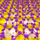
If you have a question about this talk, please contact Georg Schusteritsch. The periodicity of the elements and the non-reactivity of the inner-shell electrons are two related principles of chemistry, rooted in the atomic shell structure. Within compounds, Group I elements, for example, invariably assume the +1 oxidation state, and their chemical properties differ completely from those of the p-block elements. These general rules govern our understanding of chemical structures and reactions. Using first principles calculations, we demonstrate that under high pressure, the above doctrines can be broken. We show that both the inner shell electrons and the outer shell empty orbitals of Cs and other elements can involve in chemical reactions. Furthermore, we show that the quantized orbitals of the enclosed interstitial space may play the same role as atomic orbitals, an unprecedented view that led us to a unified theory for the recently observed high-pressure electride phenomenon. In the last example for high-pressure chemistry, we demonstrate that He can form stable compounds with ionic crystals. The driving force for these reactions is not the local chemical bonds but rather the alternation of the long-range Coulomb interactions among ions while incorporating He atoms in the lattice. Furthermore, we show the development of an efficient method that can automatically explore the surface structures by virtue of structure swarm intelligence. While applying the method on the “simple” diamond (100) surface, we discovered a hitherto unexpected surface reconstruction featuring self-assembly of carbon nanotubes (CNTs) arrays. The intriguing covalent bonding between the neighboring tubes creates a unique feature of carrier kinetics—-one dimensionality of hole states whereas two dimensionality of electron states, which may lead to novel design of superior electronics. Using very different approach, we propose and demonstrate a large family of two-dimensional semiconductors (2DSC), all adopting the same structure and consisting of only main group elements. We demonstrate the attainability of these materials, and show that they cover a large range of lattice constants, band gaps and band edge states, therefore are good candidate materials for heterojunctions. The new 2DSCs may pave a way toward fabrication of 2DSC devices at the same thriving level as 3D semiconductors. This talk is part of the Materials Modelling Seminars series. This talk is included in these lists:
Note that ex-directory lists are not shown. |
Other listsDepartment of Earth Sciences seminars Young Nanoscientist India Award Winner's Lecture sponsored by Oxford InstrumentsOther talksVisual Analytics for High-Dimensional Data Exploration and Engineering Design Thin-shell textile-reinforced concrete floors for sustainable buildings Colorectal cancer. Part 1. Presentation, Diagnosis and Intervention. Part 2. Cellular signalling networks in colon cancer and the models to study them - a basic research perspective Phylogenetic hypothesis of the Oleeae tribe (Oleaceae) Diversification and molecular evolution patterns in plastid and nuclear ribosomal DNA Coordination and inequalities in agglomeration payments: evidence from a laboratory experiment Algorithmic Investigation of Large Biological Data sets |